What happens after reset in microcontroller? How does the microcontroller boots up?
- Encode AND Decode

- Sep 6, 2024
- 16 min read
Updated: Sep 28, 2024
What Happens After Reset in STM32F407?
When the STM32F407 microcontroller is reset (either by power-on, pressing the reset button, or triggering a software reset), it doesn't directly start running your main() function. Instead, it follows a predefined sequence of steps to prepare the system for execution.
Boot Pin Check: The microcontroller first checks the state of the BOOT0 and BOOT1 pin. These pins determines the boot mode:

Startup Code Execution: After determining the boot mode, the microcontroller executes the startup code. The startup code performs these tasks:
Vector Table Setup: Sets up the vector table for exception handling and interrupt service routines.
Reset Handler: The startup code calls the Reset_Handler function, which perform these two tasks:
Copying .data Section: It copies the .data section from flash memory to SRAM.
Initializing .bss Section: It initializes the .bss section to zero.
System Initialization: Executing functions like SystemInit() to configure the system clock, PLL, and other settings.(Optional, since by default the microcontroller uses internal system clock to run which is of 16MHz in STM32F407VGT6).
Calling main(): Finally, it calls the main() function of your application code to start executing the user-defined application.
Boot Modes in STM32F407
The STM32F407 microcontroller offers three primary boot modes, and the mode selected depends on the configuration of the BOOT pins (BOOT0 and BOOT1):
Main Flash Memory Boot (Boot from Flash Memory)
In this mode, the microcontroller starts executing code from the main Flash memory, beginning at address 0x08000000.
This is the typical boot mode for most applications where the user program is stored in Flash.
System Memory Boot (Boot from System Memory)
Here, the microcontroller boots from the system memory, which holds the built-in bootloader.
The bootloader can be used to program the microcontroller via interfaces like USART, USB, CAN, etc.
System memory is mapped to start at address 0x1FFF0000.
SRAM Boot (Boot from Embedded SRAM)
In this mode, the microcontroller boots from the embedded SRAM, starting at address 0x20000000.
This mode is often handy for debugging purposes or when running code directly from SRAM.


Does the STM32 Run the Bootloader by Default, and How to Configure the BOOT Pins?
No, the STM32 does not run the bootloader by default, since the boot pins are configured so that system boot from internal flash memeroy. The boot mode that the STM32 microcontroller uses at startup is determined by the configuration of the BOOT pins (BOOT0 and BOOT1). These pins decide whether the microcontroller boots from the main Flash memory, system memory (where the built-in bootloader resides), or SRAM.
Main Flash Memory Boot (Default for Most Applications): If the BOOT pins are configured to boot from Flash memory, the microcontroller starts executing code directly from the main Flash (address 0x08000000). This is the most common configuration, where the user application is stored, and no bootloader is executed unless it’s part of the user application itself.
System Memory Boot (Bootloader Mode): To run the built-in bootloader, the BOOT pins must be configured to boot from the system memory (address 0x1FFF0000). This mode is typically used when you need to reprogram the microcontroller via interfaces like USART, USB, or CAN. In this case, the microcontroller will execute the built-in bootloader code after a reset.
SRAM Boot: This mode is used less frequently and is mainly for debugging purposes. Here, the microcontroller boots from the embedded SRAM (address 0x20000000), and no bootloader is involved unless you have specifically loaded one into SRAM.
How to Configure the BOOT Pins?
To configure the boot mode, you need to set the BOOT0 and BOOT1 pins on the STM32 microcontroller. These pins are usually configured through hardware by connecting them to either a high (VDD) or low (GND) voltage level.
BOOT 0 Pin: This pin is typically available on the microcontroller's physical package.
BOOT 1 Pin: In STM32F407 the BOOT 1 pin is connected to PB2 internally.
Common Configurations:
Boot from Main Flash Memory:
BOOT0 = 0 (GND), BOOT1 = x (don’t care)
This is the default configuration for running the user application stored in Flash memory.
Boot from System Memory (Built-in Bootloader):
BOOT0 = 1 (VDD), BOOT1 = 0 (GND)
This configuration forces the microcontroller to execute the built-in bootloader code located in system memory.
Boot from SRAM:
BOOT0 = 1 (VDD), BOOT1 = 1 (VDD)
This configuration is used for booting directly from the embedded SRAM.


Boot pins on STM32F407 development board
What is Startup Code?
Startup code is a small piece of assembly or C code that runs immediately after the microcontroller is reset or powered on. Its main purpose is to prepare the system for the execution of the main application by performing essential initialization tasks. As previously discussed the startup code is responsible for:
Vector Table Setup: Sets up the vector table for exception handling and interrupt service routines.
Reset Handler: The startup code calls the Reset_Handler function, which perform these two tasks:
Zeroing the BSS Segment: Clearing out the BSS segment where uninitialized global and static variables are stored, ensuring they start with a value of zero.
Copying Initialized Data: Copying initialized global and static variables (.data section) from Flash memory to SRAM, so they can be modified during program execution.
Calling System Initialization Functions: Executing functions like SystemInit() to configure the system clock, PLL, and other critical settings.
Jumping to the main() Function: Finally, transferring control to the main() function where the user application begins.
In an STM32CubeIDE project, the startup code is usually found in a file named startup_stm32f407xx.s. The '.s' extension indicates that it is an assembly file.
The startup code can also be written in C using compiler-Specific attributes
and inline assembly.
FLASH memory starts at address 0x80000000, where the code is stored by default. However, the microcontroller begins execution from address 0x00000000. How is it going to fetch any instruction if it is not at address 0x00000000 ?
Memory Aliasing in STM32F407
In the STM32F407 microcontroller, the memory space is organized so that the starting address 0x00000000 is aliased to different memory regions depending on the boot mode selected.
Common Memory Aliases:
0x08000000 (Flash Memory): This is where the main application code typically resides. In normal boot mode, the Flash memory at 0x08000000 is aliased to 0x00000000. This means when the processor fetches an instruction from 0x00000000, it actually accesses the Flash memory at 0x08000000.
0x1FFF0000 (System Memory): This address is where the built-in bootloader is located. If the microcontroller is configured to boot from the system memory, this area is aliased to 0x00000000.
0x20000000 (SRAM): This is the starting address of the embedded SRAM. In SRAM boot mode, the SRAM is aliased to 0x00000000.
How Does This Aliasing Work?
The aliasing is controlled by the Boot Mode settings, which are determined by the state of the BOOT0 and BOOT1 pins during reset. Based on these pins, the microcontroller maps the corresponding memory region to the starting address 0x00000000.
Boot from Main Flash Memory (BOOT0 = 0, BOOT1 = X):
Aliases 0x08000000 (Flash) to 0x00000000.
Boot from System Memory (BOOT0 = 1, BOOT1 = 0):
Aliases 0x1FFF0000 (System Memory) to 0x00000000.
Boot from SRAM (BOOT0 = 1, BOOT1 = 1):
Aliases 0x20000000 (SRAM) to 0x00000000.
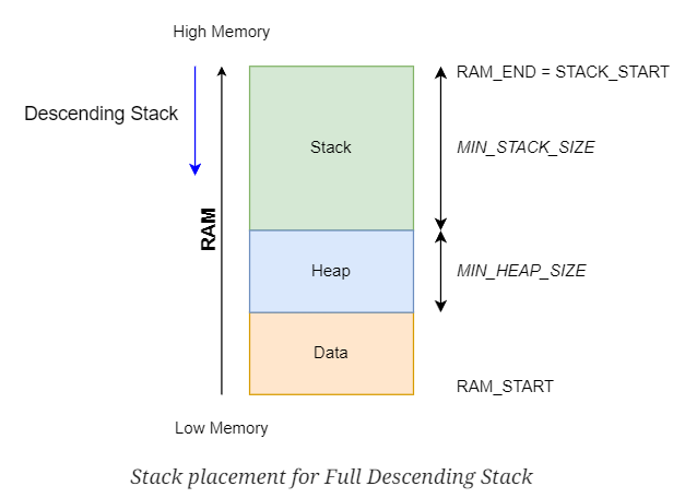
Since we are going to boot from the flash memory the cpu will fetch the instuction at the address 0x00000000 which is aliased to the address 0x80000000. The first address should contain the starting address of the Main Stack Pointer (MSP), which is essential for managing the stack during program execution.
When the microcontroller comes out of reset, the processor automatically loads the MSP with the value found at address 0x00000000.
This value represents the initial stack pointer, which points to the top of the stack in SRAM. The stack grows downward from this address.The top of the stack is define before hand in the linker script considering the size of SRAM and where to place the start of the stack.
Example:
If the initial stack pointer value stored at 0x00000000 is 0x2001FFF0, then after reset, the MSP will be set to 0x2001FFF0.
This means the top of the stack is at 0x2001FFF0, and the stack will grow downward from this address as the program executes.This is beacuse the ARM CORTEX-M4 uses fulldescending stack.
Once the MSP is initialized the program counter is loaded with the next address to be executed i.e 0x00000004.This address should contain the reset handler.
Linker Script
A linker script is a text file that provides instructions to the linker, a program that combines multiple object files generated from your source code into a single executable program. It controls how the various sections of your code and data are organized in memory.
Why Do We Need a Linker Script?
When we write a program, we typically have these:
Source Code Files: Your C/C++ files, which contain functions, variables, etc.
Object Files: Compiled versions of your source code files (produced by the compiler).
Executable Program: The final output that can be run on a microcontroller or computer.
The linker’s job is to take these object files and combine them, but it needs guidance on how to do that effectively. This is where the linker script becomes essential. It acts as a roadmap for the linker, ensuring that:
Appropriate Memory Allocation: Different types of code and data are stored in designated memory regions that align with the architecture of the microcontroller or system. For instance:
The program code (in the .text section) might need to be stored in Flash memory, which is non-volatile and retains data even when powered off.
Initialized variables (in the .data section) and uninitialized variables (in the .bss section) must be loaded into SRAM, which is volatile but provides fast read/write access during program execution.
Correct Memory Layout: The linker script defines how the various sections of your program are arranged in memory, ensuring the program has the correct layout to function as intended.
Components of a Linker Script
1. Memory Regions
This section defines the available memory regions and their properties.
Syntax:
MEMORY
{ REGION_NAME (ATTRIBUTES) : ORIGIN = START_ADDRESS, LENGTH = SIZE
}REGION_NAME: Name of the memory region (e.g., FLASH, SRAM).
ATTRIBUTES: Access permissions, such as r(read), x(execute), w(write).
ORIGIN: Starting address of the memory region.
LENGTH: Size of the memory region.
Example:
/* Memory Map */
MEMORY
{
	FLASH (rx) : ORIGIN = 0x08000000, LENGTH = 1M
	SRAM (rwx) : ORIGIN = 0x20000000, LENGTH = 128K
 }
The above statment means that the FLASH memory region is readable and executable. Its starting address is 0x08000000 and the size is 1 Mega Byte.
For SRAM starting address is 0x20000000 and the total size is 128 Kilo Bytes.
This is with respect to the data provided by the STM for STM32F407VGT6 microcontroller. See the figure below.SRAM1 + SRAM2 = 128KB which is the total size of SRAM.For FLASH memory 0x080FFFFF - 0X08000000 = 1048575 Bytes.
1048575 / 1024 = 1023.999 Kilo bytes which is ~~ 1 Mega Byte.

2. Sections
This section specifies how different parts of the code and data should be organized within the defined memory regions.
Syntax:
SECTIONS {
.section_name :
{
	*(.section_name) /* Include all sections with the name .section_name */

	(.section_name*) /* Include all sections starting with .section_name */

. = ALIGN(alignment); /*Align the next section on a specified boundary*/

symbol_name = .; /*Define a symbol with the current address*/

} > REGION_NAME
}.section_name: The name of the section (e.g., .text, .data, .bss).
*: Wildcard to include all matching sections.
ALIGN(alignment): Align the address on a specified boundary (e.g., 4 bytes).
symbol_name = . : Define a symbol representing the current address.
> REGION_NAME: Specifies where to place this section in the defined memory region.
Example:
SECTIONS
{
	.isr_vector :
	{
	   *(.isr_vector)
	}>FLASH
}
The above statements can be interpreted like this:
SECTIONS: This keyword indicates that we are defining memory sections within the linker script. Each section corresponds to a specific part of our program.
.isr_vector: This is the name of the section we’re defining. The .isr_vector section will hold the interrupt vector table.
{ ... }: The curly braces encompass the contents of the .isr_vector section. Inside these braces, we specify what should be included in this section.
> FLASH: This part specifies where to place the .isr_vector section in memory. By directing it to FLASH memory, we ensure that the interrupt vector table is stored in non-volatile FLASH memory.
*(.isr_vector): When you compile your source code files, each file generates an object file.(From .C to .O file).These object files can contain multiple sections, including .text, .data, .bss, and .isr_vector.
The statement *(.isr_vector) instructs the linker to look through all of these object files and find any section named .isr_vector.
For every object file that has a section called .isr_vector, the linker collects its contents and combines them into the output section defined in the linker script, as in this case it will be stored in the FLASH.
SInce we had already defined the starting address of FLASH as 0x08000000 (FLASH (rx) : ORIGIN = 0x08000000, LENGTH = 1M) and the first SECTION we defined is the .isr_vector, therefore the contents of .isr_vector will be stored at the starting address.
So when microcontroller boots up the first data it will encounter will be the vector table which we will have to define in the startup code.In the vector table we will need to define the addresses of the different ISR's.
We will talk about the vector table in detail in the Startup code section.
Below is the complete SECTION command defined.
/* Sections */
SECTIONS
{
	.isr :
	{
	   *(.isr_vector)
	}>FLASH

	.text :
	{
	  *(.text)
	  *(.rodata)
	  _etext = .;
	}>FLASH

	.data :
	{
	  _sdata = .;
	  *(.data)
	  _edata = .;
	}>SRAM AT >FLASH

	.bss :
	{
	 _sbss = .;
	 *(.bss)
	 _ebss = .;
	}>SRAM
}.text: This is the name of the section being defined similar to .isr_vector.
(.text): This line instructs the linker to include all sections named .text from all input object files. The * acts as a wildcard, meaning it will find any .text section in the specified object files.
*(.rodata): Similarly, this line includes all sections named .rodata (read-only data), which usually contains constant variables or string literals that should not be modified during execution.
Symbols: in a linker script represent addresses or locations in memory. Symbols can be used to reference memory addresses in various sections.They can be defined using the following syntax:
mysymbol = .; // Defines a symbol called my_symbol at the current location (.)Location Counter (.) : Represents the current location in memory.
etext = .;: This line defines a symbol etext that represents the current location (.) in memory right after all the .text and .rodata sections have been included. This symbol can be used in the application code to determine where the executable code ends in memory.This will be required when writing the startup code.
> FLASH: This indicates that the .text section and its contents should be placed in the FLASH memory region. The FLASH region is defined earlier in the linker script and typically corresponds to the memory area where your microcontroller's firmware is stored.
Explanation of >SRAM AT >FLASH in the .data section
When the program starts:
The microcontroller boots up and runs the code in its FLASH memory, where the firmware is stored. (AT >FLASH)
The AT >FLASH directive indicates that the linker should place the initial values of these variables in FLASH so that they can be copied to SRAM at runtime.
Copying from FLASH to SRAM:
The .data section usually contains initialized global and static variables. When the program starts, the startup code (often found in the Reset_Handler) will copy the data from FLASH to the SRAM.
Linker Script Complete Code
/* 	Entry Point */
ENTRY(Reset_Handler)

/* Memory Map */
MEMORY
{
	FLASH(rx)   : ORIGIN = 0x08000000, LENGTH = 1024K
	SRAM(rwx)   : ORIGIN = 0x20000000, LENGTH = 128K
}

/* Sections */
SECTIONS
{
	.isr_vector :
	{
	   *(.isr_vector)
	}>FLASH

	.text :
	{
	  *(.text)
	  *(.rodata)
	  _etext = .;  /* End of .text section */
	}>FLASH

	.data :
	{
	  _sdata = .;  /* Start of .data section */
	  *(.data)
	  _edata = .;  /* End of .data section */
	}>SRAM AT >FLASH

	.bss :
	{
	 _sbss = .;
	 *(.bss)
	 _ebss = .;
	}>SRAM
}
Entry Point: The ENTRY(Reset_Handler) directive specifies that the program should start execution at the address labeled Reset_Handler. This is typically where the system initialization code resides.
How to write a startup code ?
Startup code contains these 3 things:
Vector Table Placement in Code Memory: The vector table is located at the start of the code memory space at address 0x08000000.
Reset Handler Initialization: The Reset Handler is responsible for copying the .data section from FLASH to SRAM and to intialize the .bss section to 0.
Calling main(): Once initialization is complete, the Reset Handler calls the main() function to start the application.
Implementing a vecor table
The vector table in a microcontroller is essentially an array of addresses, where each address points to a specific Interrupt Service Routine (ISR) function.
When an interrupt or exception occurs, the microcontroller uses the vector table to find the address of the corresponding ISR and then jumps to that address to execute the ISR.
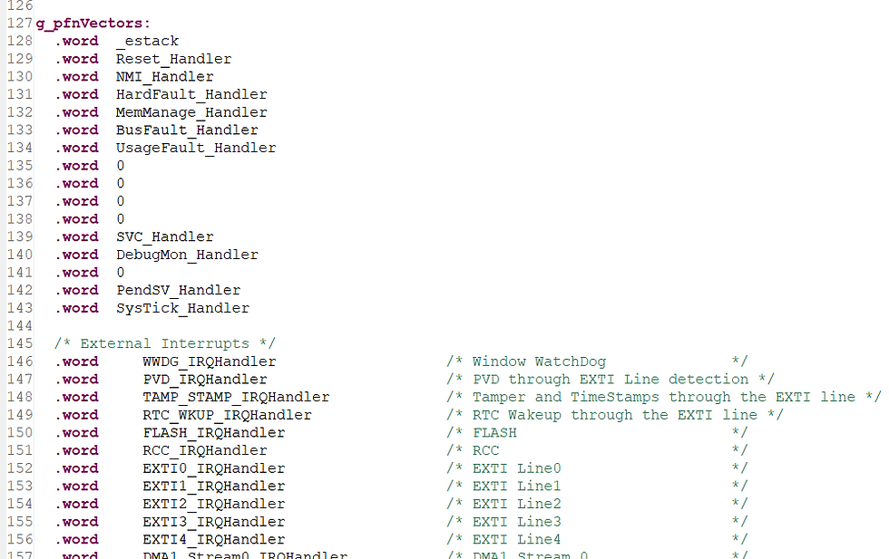
The above diagram shows vector table written in assembly in the startup code generated by the STM32CUBE IDE.The first enrty '_estack' is for intialising the Main Stack Pointer and the second entry is the 'Reset_Handler' from where the main() function will be called.
Startup code in C:
Writing a Vector Table :
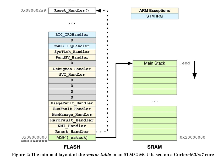
The above figure shows the vector table placment in the memory.The first entry should be the MSP, the second should be the reset handler and so on.
/* Vector Table */
#include <stdint.h>

#define SRAM_START	0x20000000
#define SRAM_END       0x2001FFFF
#define STACK_START    0x2001FFFF

void Reset_Handler(void);

__attribute__((section(".isr_vector"))) uint32_t Vectors[] = {
    STACK_START,
    (uint32_t)&Reset_Handler
};
In the above program we have set the end address of SRAM 2 as the Stack Starting point (0x2001FFFF).This is beacuse the stack in ARM Cortex-M4 is a full descending stack.In ARM Cortex-M4, the stack grows downwards, which means that the stack pointer starts at a higher memory address and decreases as data is pushed onto the stack. This is called a full descending stack, where the stack pointer (SP) initially points to the highest valid address of the stack region, and as the stack grows, it moves towards lower addresses.
In the program, STACK_START is defined as 0x2001FFFF, which is the last valid address in the SRAM (ending address of the SRAM). When the microcontroller starts, the stack pointer is initialized to this value, and the stack grows downwards from this point.
The Vector Table includes this STACK_START value as the first entry, which is loaded into the Main Stack Pointer (MSP) during startup. This ensures that when the system begins executing, it has a properly initialized stack to handle function calls, interrupts, and other operations that rely on stack space.
After the stack pointer is initialized, the microcontroller fetches the address of the Reset_Handler from the second entry in the vector table and jumps to it. The Reset_Handler typically takes care of system initialization tasks, such as setting up memory and calling the main() function.
/* Implementation of Reset Handler */

extern uint32_t _etext;
extern uint32_t _sdata;
extern uint32_t _edata;
extern uint32_t _sbss;
extern uint32_t _ebss;

void Reset_Handler(void) {
    /* Copy the .data section from Flash to SRAM */

    uint32_t* src = &_etext; // End of .text section in Flash
    uint32_t *ptr = &_sdata; // Start of .data section in SRAM
    while (ptr < &_edata)
    {
        *ptr++ = *src++;       // Copy data
    }

     /* Clear the .bss section */
    uint32_t* p = &_sbss;
    while (p < &_ebss)
    {
        *p++ = 0;  // Set each word to zero
    }

    main();
}
The first part of the Reset_Handler function handles copying the initialized variables (the .data section) from Flash to SRAM.
_etext is a symbol (generated by the linker) that marks the end of the .text section (code and read-only data) in Flash. Right after _etext, the initialized data is stored in Flash.
_sdata and _edata are symbols representing the start and end of the .data section in SRAM.
The loop iterates through each word (32-bit chunk) of initialized data, copying it from Flash to SRAM, so that the program can use it.
The second part of the Reset_Handler function handles the .bss section. The .bss section is where uninitialized global and static variables are stored. By convention, the C standard expects uninitialized variables to be zeroed out before the program starts. In this part of the code:
_sbss and _ebss are symbols representing the start and end of the .bss section in SRAM.
The loop sets every word in the .bss section to zero.
Finally the Reset_Handler calls the main() function.
Full source code of Startup code
/*Startup Code */

#include <stdint.h>

#define SRAM_START      0x20000000
#define SRAM_END        0x2001FFFF
#define STACK_START     0x2001FFFF

extern uint32_t _etext;
extern uint32_t _sdata;
extern uint32_t _edata;
extern uint32_t _sbss;
extern uint32_t _ebss;

void main(void);
void Reset_Handler(void);

__attribute__((section(".isr_vector"))) uint32_t Vectors[] = {
    STACK_START,
    (uint32_t)&Reset_Handler
};

void Reset_Handler(void) {
    // Copy the .data section from Flash to SRAM
    uint32_t* src = &_etext; // End of .text section in Flash
    uint32_t *ptr = &_sdata;              // Start of .data section in SRAM
    while (ptr < &_edata)
    {
        *ptr++ = *src++;       // Copy data
    }

     // Clear the .bss section
    uint32_t* p = &_sbss;
    while (p < &_ebss)
    {
        *p++ = 0;  // Set each word to zero
    }

    main();
}
The above code is the basic structure of a startup code.We haven't implemented the other ISR functions.This one will be enough to make the porgram to jump into the main code.We could write program to toggle the LED in the main() to see that the board actually boots up.Inorder to use interrupts we will have to declare the ISR functions and populate the vector table with the address of these ISR.A complete source code link(Github link) is attached at the end of this post.
main() Source Code
/*
* To toggle LED connected to PD12 and PD14 of STM32F407 Discovery Board
*Steps:
*Enable clock access to GPIOD
*Set PD12 AND PD14 as output
*Set ODR12 and ODR14 to 1(Turn ON)
*Call delay()
*Set ODR12 and ODR14 to 0(Turn OFF)
*/

#include <stdint.h>
void delay(void);
// RCC AHB1ENR base address
#define AHB1_BASE                  0x40020000U
#define RCC_BASE                   (AHB1_BASE + (0x3800U))
#define RCC_AHB1ENR                (uint32_t *)(RCC_BASE + (0x30U))
#define GPIOD_CLOCK_EN             (1U << 3U)
#define GPIOD_BASE                 (AHB1_BASE + (0x0C00U))
#define GPIOD_MODER                (uint32_t *)(GPIOD_BASE + (0x00U))
#define PD12_BIT_24_EN             (1U << 24U)
#define PD12_BIT_25_DISABLE        (~(1U << 25U))
#define PD14_BIT_28_EN             (1U << 28U)
#define PD14_BIT_29_DISABLE        (~(1U << 29U))
#define GPIOD_ODR                  (uint32_t *)(GPIOD_BASE + (0x14U))
#define PD12_OUTPUT_EN             (1U << 12U)
#define PD12_OUTPUT_DISABLE        (~(1U << 12U))
#define PD14_OUTPUT_EN             (1U << 14U)
#define PD14_OUTPUT_DISABLE        (~(1U << 14U))

int main(void)
{
    uint32_t *gpiod_clock, *gpiod_moder, *gpiod_odr;
    gpiod_clock = RCC_AHB1ENR;
    //Clock for GPIOD enabled
    *gpiod_clock |= GPIOD_CLOCK_EN;
     gpiod_moder = GPIOD_MODER;
    //PD12 set as output
    *gpiod_moder |= PD12_BIT_24_EN;
    *gpiod_moder &= PD12_BIT_25_DISABLE;
    //PD14 set as output
    *gpiod_moder |= PD14_BIT_28_EN;
    *gpiod_moder &= PD14_BIT_29_DISABLE;
     gpiod_odr = GPIOD_ODR;
     while (1)
    {
        //PD12 and PD14 set
        *gpiod_odr |= PD12_OUTPUT_EN;
        *gpiod_odr |= PD14_OUTPUT_EN;
        delay();
        //PD12 and PD14 reset
        *gpiod_odr &= PD12_OUTPUT_DISABLE;
        *gpiod_odr &= PD14_OUTPUT_DISABLE;
        delay();
    }
    return 0;
}

void delay(void)
{
    for (volatile int i = 0; i < 400000; i++);
}
1. Enable Clock Access to GPIO Port D
Every peripheral in STM32 requires a clock to function. The clock for GPIO Port D must be enabled before configuring any of its pins.
STM32 peripherals, including GPIO, are controlled by the RCC (Reset and Clock Control) module.
The RCC has specific registers to control the clock for different peripherals. To enable the clock for GPIO Port D, you will need to set the 3rd bit in the AHB1 peripheral clock enable register (RCC_AHB1ENR).
2. Configure PD12 and PD14 as Output Pins
Once the clock is enabled, you need to configure the mode of PD12 and PD14 pins to output mode. This is done by configuring the MODER (Mode Register) of GPIO Port D.
Each GPIO pin has two bits in the MODER register that define its mode. For each pin, you can configure it as input, output, alternate function, or analog.
To set PD12 and PD14 as output pins, you need to:
Set 24th and 28th bit to 1 and 25th and 29th bit to 0.
3. Control the Output Data Register (ODR)
After configuring the pins as outputs, you can control the Output Data Register (ODR) to toggle the state of PD12 and PD14.
The ODR register controls the state of the pins configured as outputs.
Each pin has a corresponding bit in the ODR register. Writing a 1 to a pin's bit in the ODR will turn it ON (set it HIGH), and writing a 0 will turn it OFF (set it LOW).
To toggle the LEDs connected to PD12 and PD14:
Set the 12th and 14th bits in the ODR to 1 to turn them ON.
After a delay, reset the bits in the ODR to 0 to turn them OFF.
This cycle repeats to create a toggling effect.


Comments