Understanding GPIO Pin Toggling in STM32F407
- Encode AND Decode

- Sep 3, 2024
- 3 min read
What is GPIO?
GPIO stands for General Purpose Input/Output which are the pins through which microcontroller talks and listens to the outside world. We can use them to read input signals or control output devices like LEDs, buttons, sensors, etc.
In STM32F407, there are a bunch of GPIO ports labeled from GPIOA to GPIOI, each having 16 pins.To control these pins, we have several registers. Registers are just special memory locations that control different aspects of the GPIO pins.
GPIO Registers
GPIO Mode Register (MODER)
Function: The MODER register is used to set the mode of each GPIO pin. Each pin has two bits in this register, allowing you to configure it as input, output, alternate function, or analog mode.
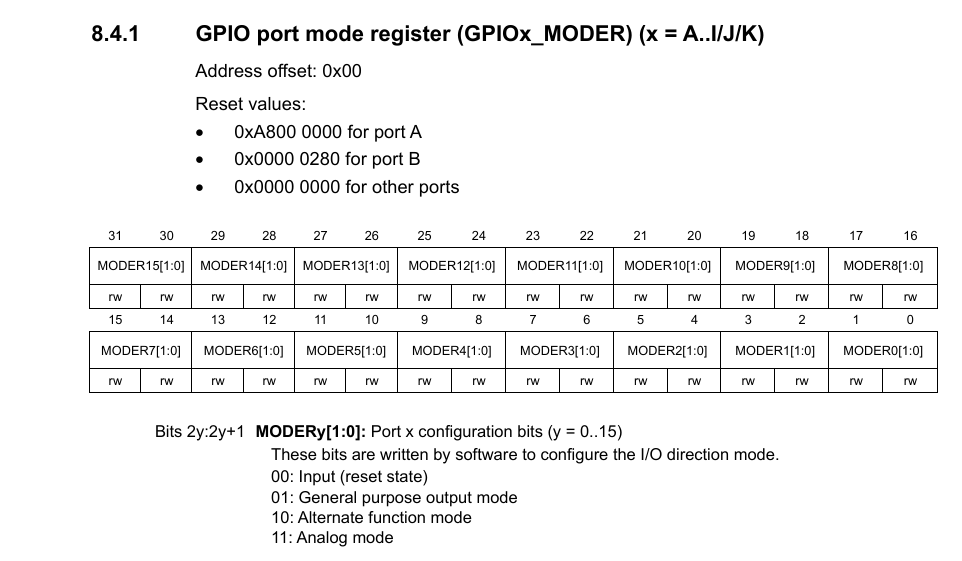
Configuration Options:
00: Input Mode – The pin is configured to read input signals.
01: Output Mode – The pin is configured to output digital signals.
10: Alternate Function Mode – The pin is used by another peripheral (like USART, SPI, etc.).
11: Analog Mode – The pin is configured for analog input/output, typically used for ADC or DAC functions.
Example Configuration:
If you want to set pin 12 of GPIO port D (PD12) to output mode, you would modify the corresponding bits in the MODER register.
//Setting PD12 as Output
GPIOD->MODER |= (1 << 24); //Set 24th bit as one
GPIOD->MODER &= ~(1 << 25); //clear 25th bit

//You can also use macro defined in the CMSIS
GPIOD->MODER |= (GPIO_MODER_MODER12_0); //Set 24th bit as one
GPIOD->MODER &= ~(GPIO_MODER_MODER12_1); //clear 25th bit
GPIO Output Data Register (ODR)
Function: The ODR register controls the output state of the GPIO pins configured as outputs. Each bit in this register represents the output state of one pin.

Configuration Options:
0: The pin is driven low.
1: The pin is driven high.
Example Configuration:
If you want to set pin 12 of GPIO port D (PD12) to high, set corresponding bit ODR12 as 1.
//Setting PD12 as High
GPIOD->ODR |= (1 << 12);

//You can also use macro defined in the CMSIS
GPIOD->ODR |= GPIO_ODR_ODR_12;
GPIO Bit Set/Reset Register (BSRR)
Function: The BSRR register allows for atomic setting or resetting of GPIO pins.
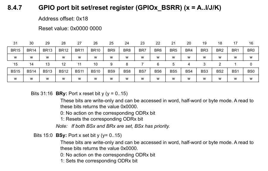
Writing 1 to a bit in the lower 16 bits sets the corresponding pin, while writing 1 to a bit in the upper 16 bits resets it.
//Setting PD12 as High
GPIOD->BSRR |= (1 << 12);

//You can also use macro defined in the CMSIS
GPIOD->BSRR = GPIO_BSRR_BS12;
While there are additional registers available for modifying GPIO pins, we'll focus exclusively on the registers necessary for toggling the LED at this time.
Toggling LED connected to PD12 on STM32F407 Discovery Board
Enable the Clock for GPIO Port D:
Activate the clock for GPIO port D to allow access to its registers.
Configure PD12 as an Output:
Set the mode of PD12 to output by configuring the relevant bits in the GPIO port D mode register.
Set the Output Type (Optional):
Choose the output type for PD12, which can be push-pull (default) or open-drain, by configuring the output type register if needed.
Set the Output Speed (Optional):
Define the output speed (e.g., low, medium, high) for PD12 by configuring the output speed register if necessary.
Configure Pull-Up/Pull-Down Resistors (Optional):
Set the pull-up or pull-down resistors for PD12, if required, by configuring the pull-up/pull-down register.
Toggle PD12:
Change the state of PD12 by writing to the output data register (ODR) or using the bit set/reset register (BSRR) to set or clear the pin. This will switch the pin between high and low states.Also add delay to observe the toggling effect.
Source Code
#include "stm32f407xx.h"

void clock_config(void);
void gpio_config(void);
void delay(void);

int main(void) {
    clock_config();
    gpio_config();
    while (1) {

        // Set PD12 high
        GPIOD->BSRR = GPIO_BSRR_BS12;
        delay();

        // Set PD12 low
        GPIOD->BSRR = GPIO_BSRR_BR12;
        delay();
    }
}

// Enabling clock access to the GPIOD
void clock_config(void) {
    // Setting 3rd bit in the RCC_AHB1ENR register.
    RCC->AHB1ENR |= RCC_AHB1ENR_GPIODEN;
}

// Setting MODE register to output type
void gpio_config(void) {
    // GPIOD pin 12 set to output.
    GPIOD->MODER |= GPIO_MODER_MODER12_0;
    GPIOD->MODER &= ~(GPIO_MODER_MODER12_1);
}

// Function to generate time delay
void delay(void) {
    int i = 0;
    for (i = 0; i < 70000; i++);
}


Comments